Introduction to CVD method for graphene production
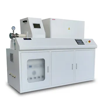
Chemical Vapor Deposition (CVD) is a widely adopted method for the production of high-quality graphene. This method involves the use of a substrate, which is usually made of copper, and a carbon-containing gas, such as methane or ethylene. The gas is then heated to a high temperature, and the carbon atoms are deposited onto the substrate, forming a layer of graphene. The CVD method is advantageous because it allows for the production of large-area graphene films, with excellent uniformity and high quality. However, the process is challenging and requires careful control of the growth parameters, such as temperature, gas flow rate, and pressure, to ensure the production of high-quality graphene.
Table of Contents
CVD Process and Its Benefits
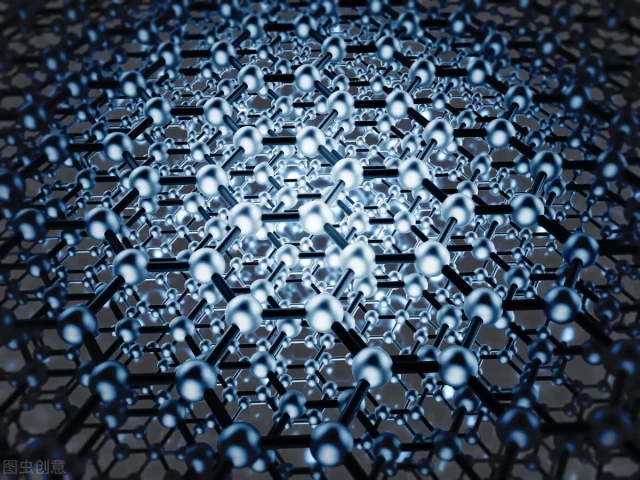
Chemical Vapor Deposition (CVD) is a widely used technique for the synthesis of graphene, a material known for its outstanding electronic, thermal, and mechanical properties. CVD has enabled the production of large-scale sheets of graphene, which are atomically thin sheets of hybridized carbon atoms arranged in a honeycomb structure. The CVD process involves the deposition of gaseous reactants onto a substrate. The graphene is grown on a metallic surface like Cu, Pt or Ir, after which it can be separated from the metal and transferred to specifically-required substrates.
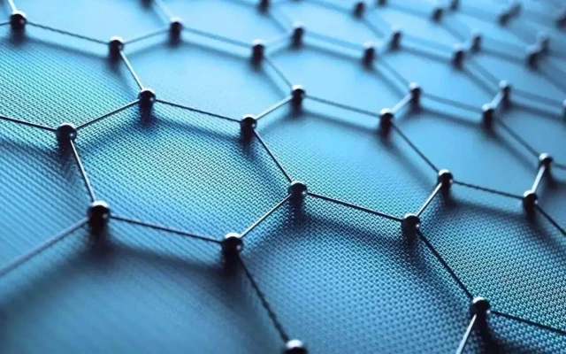
The CVD process can be controlled by adjusting various parameters such as temperature, pressure, duration of time, and many more. The high-quality graphene produced by CVD exhibits common characteristics such as high homogeneity, imperviousness, high purity, fine grains, and good control over layer number.
One of the main advantages of the CVD process is that the chemical reactants are gases that take advantage of the physical characteristics of how gases flow over the substrate surface to build uniform, highly conformal films on irregularly shaped surfaces. This can result in a more controllable surface morphology for many applications.
CVD offers a wide variety of coating materials based on metals, alloys, and ceramics. The chemical reactions that characterize CVD can also be used to form alloys. It can provide an easily scalable and controllable process for many types of batch production runs that provide major cost savings with economies of scale.
CVD deposits very pure films, over 99.995% purity. They are typically fine-grained and can be used to enable a very high degree of hardness such as Diamond-like Carbon (DLC) coatings. CVD is also known for its ability to yield high-quality graphene sheets with a low defect count and good uniformity.
CVD usually doesn't require as high a vacuum as PVD processes, or any vacuum at all. Except for the chemical byproducts that result from the reactions at the outflow, CVD equipment for the most part is self-cleaning. This makes it an attractive option for many industries, including the semiconductor and optoelectronics industries.
In conclusion, the CVD process of graphene synthesis has several benefits, including its ability to produce large-scale sheets of graphene suitable for industrial applications, its flexibility to grow graphene on a wide range of substrates, its scalability for batch production runs, and its ability to produce high-quality, uniform graphene films.
CVD Graphene Challenges and Limitations
Chemical Vapor Deposition (CVD) is a highly popular method for synthesizing high-quality graphene at an industrial scale. However, the process also has its own set of challenges and limitations.
Equipment Cost
One of the primary challenges of CVD graphene is the high cost of the equipment required to produce it. The process requires high temperatures and precise control of the gas flow and reaction parameters, which can be difficult to achieve and maintain.
Substrate Quality
The quality of the graphene produced can be affected by the substrate used, which can result in defects or impurities. This can impact the performance of the graphene in various applications.
Scalability
Another limitation of CVD graphene is its scalability. While it is possible to produce large sheets of graphene using this method, the process becomes more difficult and expensive as the size of the sheet increases.
Environmental Impacts
The production of CVD graphene can also have negative environmental impacts due to the use of hazardous chemicals and energy-intensive processes. This is a significant concern, especially given the increasing demand for high-quality graphene in various applications.
Despite these challenges, solutions are being developed to overcome these limitations.
New Substrates
Researchers are exploring new substrates that can improve the quality and consistency of CVD graphene. This can potentially address the issue of substrate quality and improve the performance of graphene in various applications.
Efficient and Cost-effective Equipment
Researchers are developing more efficient and cost-effective equipment and processes that can make the production of CVD graphene more accessible and environmentally friendly. This can help reduce the equipment cost and environmental impact of CVD graphene production.
In conclusion, while CVD graphene faces certain challenges and limitations, it is still widely considered as an important and promising method to produce graphene. The demand for high-quality graphene continues to grow, and solutions are being developed to overcome the limitations of CVD graphene production. It is likely that these solutions will play an important role in the future of CVD graphene synthesis.
Market Status of CVD Graphene
CVD graphene has gained significant market status due to its unique properties, including its high electrical conductivity, high mechanical strength, and transparency. The market for CVD graphene is expected to grow significantly in the coming years, driven by the increasing demand for advanced materials with unique properties.
Increasing Demand for Advanced Materials
As the demand for advanced materials with unique properties increases, the market for CVD graphene is expected to grow. CVD graphene has several unique properties, including its high electrical conductivity, high mechanical strength, and transparency. These properties make it an ideal material for use in a variety of applications, including electronics, energy storage, and biomedical devices.
Wide Range of Applications
CVD graphene is used in a variety of applications, including electronics, energy storage, and biomedical devices. In the electronics industry, CVD graphene is used in the production of high-performance transistors, touchscreens, and other electronic components. In the energy storage industry, CVD graphene is used in the production of supercapacitors, batteries, and other energy storage devices. In the biomedical industry, CVD graphene is used in the production of biosensors, drug delivery systems, and other biomedical devices.
Potential for Large-Scale Production
CVD graphene has the potential to be produced on a large scale, making it an attractive option for manufacturers. The CVD process is reasonably straightforward, although some specialist equipment is necessary, and in order to create good quality graphene, it is important to strictly adhere to guidelines set concerning gas volumes, pressure, temperature, and time duration. With ongoing research and development efforts, it is likely that the challenges associated with CVD graphene will continue to be addressed, leading to further improvements in the quality and uniformity of the material.
Conclusion
In conclusion, the market for CVD graphene is expected to grow significantly in the coming years, driven by the increasing demand for advanced materials with unique properties. CVD graphene has several unique properties, including its high electrical conductivity, high mechanical strength, and transparency, making it an ideal material for use in a variety of applications. With ongoing research and development efforts, it is likely that the challenges associated with CVD graphene will continue to be addressed, leading to further improvements in the quality and uniformity of the material, and making it an even more attractive option for manufacturers.
Chemical Vapor Deposition Techniques for Graphene Production
Chemical Vapor Deposition (CVD) is one of the most widely used techniques for the synthesis of graphene-based materials. The CVD growth of graphene involves activated chemical reactions of precursors in a specially-designed environment. The characteristic processing parameters (pressure, temperature, precursor nature, gas flow state, wall/substrate temperature, depositing time, and activation manner) determine the final quality of the graphene.
Precursors for CVD Growth of Graphene
A range of precursors has been previously reported as suitable for the growth of graphene in the CVD reactor. Gaseous carbon sources, such as methane (CH4) gas, are the most widely used carbon precursor and are introduced to the reaction chamber by a gas delivery system. Solid precursors may be directly loaded into the reactor chamber, while liquid carbon sources evaporated into the vapor phase are introduced into the CVD reactor using bubblers.
Substrates for CVD Growth of Graphene
Transition metals can work as both synthesizing substrates and catalysts and are relatively cheap compared with noble and rare-earth metals. Among the most widely used substrates for graphene growth via CVD are copper, nickel, and cobalt. Copper surfaces are regarded as superior substrates, since graphene monolayers can be deposited exclusively. Nickel surfaces have turned out to support the formation of controlled graphene layers. Other transition metals, such as ruthenium, iridium, platinum, rhodium, gold, palladium, and rhenium have also been investigated as potential substrates for CVD growth of graphene.
Methods for CVD Growth of Graphene
The CVD methods can be categorized into seven main types based on temperature, pressure, wall/substrate, nature of precursor, depositing time, gas flow state, and activation/power source. Thermal CVD on metals was first reported in 1966 to grow highly crystalline graphite films on Ni substrates. Later, deposition of a single layer of graphite was conducted using a CVD method on Pt surface by the hydrocarbon decomposition. Following the first isolation of graphene in 2004, the study of CVD’s potential for growing graphene films was successfully achieved by using low-pressure CVD (LPCVD) to grow graphene on Ir.
Challenges and Solutions
The production of graphene using CVD poses several challenges, such as the control of the growth process, the uniformity of the film, and the scalability of the process. The most significant challenge of CVD is the control of the nucleation and growth of graphene on the substrate. This requires precise control of the temperature, pressure, and gas flow during the deposition process. The uniformity of the graphene film across a large area is also a challenge, as the growth rate can vary across the substrate. Furthermore, the scalability of the process is a concern, as the production of large-area graphene films requires a high degree of control over the deposition process.
Several solutions have been proposed to address these challenges. One approach is to optimize the growth parameters, such as the temperature, pressure, and gas flow, to achieve uniform and high-quality graphene films. Another solution is to use a two-step process, where a thin layer of metal is deposited on the substrate first, followed by the deposition of graphene on top. This approach can improve the control of nucleation and growth and increase the uniformity of the film. Additionally, the use of advanced techniques, such as plasma-enhanced CVD, can improve the scalability of the process and enable the production of large-area graphene films.
Techniques for High-Quality CVD Graphene Production
Optimization of Deposition Parameters
Achieving uniformity and control over the thickness of CVD graphene is a major challenge. To address this challenge, the deposition parameters need to be optimized. Temperature, pressure, and precursor concentration are the most critical parameters that affect the quality of graphene. The optimization of these parameters can improve the uniformity and thickness of the graphene produced.
Post-Treatment Methods
The formation of defects, such as wrinkles and tears, during the growth process, is another challenge of CVD graphene production. To overcome this, various post-treatment methods have been developed to repair the defects and improve the quality of the graphene. Thermal annealing and chemical functionalization are the most commonly used post-treatment methods.
Substrate Selection
The selection of the substrate plays a critical role in CVD graphene production. The substrate must be able to withstand high temperatures and provide a smooth and clean surface for the graphene to grow on. Silicon carbide (SiC) and copper (Cu) are commonly used substrates due to their thermal stability and smooth surface properties.
Scalability of the CVD Process
To enable large-scale graphene production, continuous roll-to-roll CVD processes have been developed, which utilize flexible substrates and enable high throughput production. This process is an advancement, as it has enabled mass production of high-quality graphene films, which is important for the commercialization of graphene-based products.
In conclusion, the optimization of deposition parameters, post-treatment methods, substrate selection, and scalability of the CVD process are essential for the production of high-quality CVD graphene. These techniques and solutions have been developed to overcome the challenges of CVD graphene production and produce high-quality graphene for use in a wide range of applications.
Prodotti correlati
- Utensili di ravvivatura per diamante CVD per applicazioni di precisione
- Fornace Tubolare per CVD Multi Zone Macchina Deposizione Chimica da Vapore Sistema Camera Attrezzatura
- Cupole di Diamante CVD per Applicazioni Industriali e Scientifiche
- Diamante CVD per applicazioni di gestione termica
- Sistema di Apparecchiature per la Deposizione Chimica da Vapore CVD Camera a Scorrimento Forno a Tubo PECVD con Gassificatore di Liquidi Macchina PECVD
Articoli correlati
- Come verificare se il vostro diamante è prodotto con la tecnica CVD
- Vantaggi e svantaggi della deposizione chimica da vapore (CVD)
- Diamante CVD:Materiale superiore per finestre ottiche
- Metodi di rivestimento per la crescita di film di cristallo singolo
- Panoramica completa delle tecnologie di deposizione da vapore chimico (CVD)
